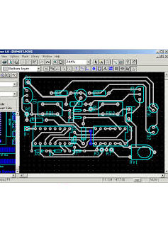
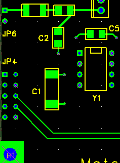
PCB Design Layout
 Vnisource offers full design support to the electronics industry. Our staffs have
strong background that understand today’s requirements in “Design for Manufacturing”
(DFM), “Design for Assembly” (DFA) and “Design for Testability” (DFT). Vnisource offers full design support to the electronics industry. Our staffs have
strong background that understand today’s requirements in “Design for Manufacturing”
(DFM), “Design for Assembly” (DFA) and “Design for Testability” (DFT).
Vnisource supports every aspect of PCB engineering, from design layout and drafting
through finished documentation. We provide complete support of R & D meeting a wide
range of electrical engineering needs. We can convert Thru-hole to surface mount and
wire wrap to PCB’s. Our staffs have the experience to design and drafting from DC to
1 GHZ in the RF environment and High Speed Digital for today’s complex boards
including Ball Grid Array (BGA).
Design Layout Capabilities:- Signal Integrity: Analog, Digital and RF
- High Speed, Controlled Impedance
- Micro Ball Grid Array (BGA)
- Microvias, Fine Pitch, High Density
- Manual, Auto, or Interactive Routing
- Single to Multi-Layer Layout
- Thru-hole to Surface Mount Conversion
- Wire Wrap to Production PCB Conversion
- Drawings per IPC-D-325, Mil-Std or Customer Spec
- Eletro Mechanical Layout and Detailing
- Gerber / Excellon CAD file generation
Our CAD/PCB Software Toolset:- ORCAD CAPTURE CIS/LAYOUT(Cadence)
- CONCEPT HDL/ALLEGRO (Cadence)
- SPECCTRA ROUTER (Cadence)
- SPECCTRA QUEST(Cadence)
- POWERLOGIC/POWERPCB (Mentor Graphics)
- CAM350(DownStream)
- P-CAD 200x PCB/SCH(ACCEL/Altium)
- GERBTOOL(Wise Software)
- AUTOCAD/MECHANICAL DESKTOP(AutoDesk)
- SOLIDWORKS
Tradition Design Outputs:- Design Database File
- Gerber Files
- NC Drill Files
- Fab Drawings
- Assembly Files
- ATE Files
- IPC-356 Files
(In addition, we have the capability to produce virtually any output requirement.)
Back to top
High-Speed PCB Design
Your Problem
High-speed PCB design is facing its toughest challenges ever today. Board speeds
are commonly over 100 Mhz, and components are switching in the nanosecond range.
Signal integrity has become a greater concern. And the pressures to cut time-to-market
and development costs (shorter project cycle times and less design iterations)
are increasing.
Our Solution
The approach we used for handling high-speed designs is the physical constraints
methodology. First your EE converts the electrical requirements for the design into
physical rules. We use these rules to enter into our PCB design database and adhered
to during placement and routing of the design.
In addition we use tools that are specific to high-speed PCB design. These tools
truly integrate the electrical and physical worlds, allowing the design process
to be driven directly by your electrical rules. Throughout the process - from parts
placement through routing - there is interactive real-time signal integrity analysis
and comparison of the physical design to your electrical design requirements and
constraints.
Vnisource staffs have the sophisticated signal integrity knowledge and experience
required for your high-speed PCB design. Let us show you how we can help with your
next project.
Back to top
|